


MTW European Type Trapezium Mill
Input size:30-50mm
Capacity: 3-50t/h
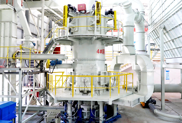
LM Vertical Roller Mill
Input size:38-65mm
Capacity: 13-70t/h
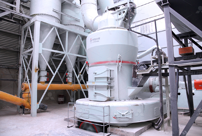
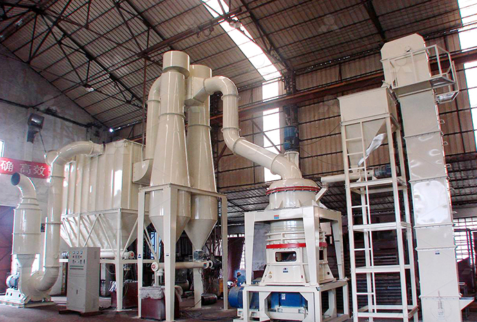
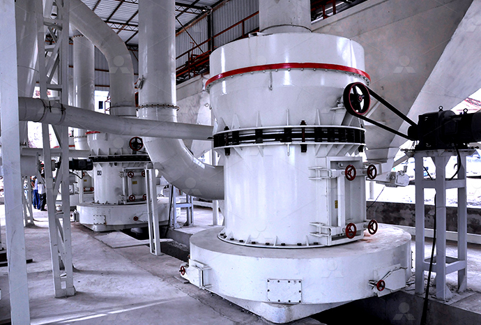
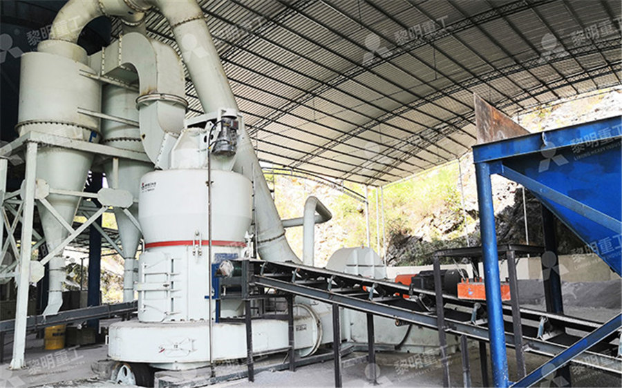
Raymond Mill
Input size:20-30mm
Capacity: 0.8-9.5t/h
Sand powder vertical mill
Input size:30-55mm
Capacity: 30-900t/h
LUM series superfine vertical roller grinding mill
Input size:10-20mm
Capacity: 5-18t/h
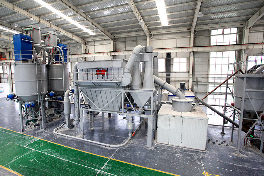
MW Micro Powder Mill
Input size:≤20mm
Capacity: 0.5-12t/h
LM Vertical Slag Mill
Input size:38-65mm
Capacity: 7-100t/h
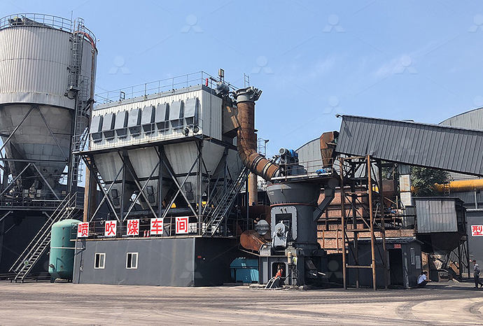
LM Vertical Coal Mill
Input size:≤50mm
Capacity: 5-100t/h
TGM Trapezium Mill
Input size:25-40mm
Capacity: 3-36t/h

MB5X Pendulum Roller Grinding Mill
Input size:25-55mm
Capacity: 4-100t/h
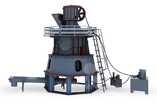
Straight-Through Centrifugal Mill
Input size:30-40mm
Capacity: 15-45t/h
Single crystal silicon Sand Requirements
.jpg)
710: Semiconductor Grade Silicon Chemistry LibreTexts
Electronicgrade silicon is also known as semiconductorgrade silicon (SGS) In order for the purity levels to be acceptable for subsequent crystal growth and device fabrication, EGS must have carbon and oxygen impurity levels less Electronicgrade silicon (EGS), a polycrystalline material of high purity, is the starting material for the preparation of single crystal silicon EGS is made from metallurgicalgrade silicon (MGS) 2 Crystal Growth and Wafer Preparation City University of Hong 2022年4月13日 This chapter provides an overview of the electronic and mechanical characteristics of silicon and describes the major steps required to manufacture silicon wafers: Silicon Properties and Crystal Growth SpringerLink2024年1月9日 A Single Crystal Ingot The next step is to grow a single crystal ingot from the purified silicon Why single crystal? This atomic alignment provides superior semiconducting properties essential for integrated circuits The most Silicon Wafer Material: From Sand to Semiconductors

Monocrystalline silicon Wikipedia
Monocrystalline silicon, often referred to as singlecrystal silicon or simply monoSi, is a critical material widely used in modern electronics and photovoltaics As the foundation for siliconbased discrete components and integrated circuits, it 2024年9月7日 The process begins with the production of highpurity silicon ingots through the Czochralski or Float Zone method: a Czochralski method to Produce Silicon Ingots In the Czochralski method, a seed crystal is dipped Silicon Wafer Manufacturing Process: Sand to Silicon2017年1月1日 The starting material for highpurity silicon single crystals is silica (SiO 2) The first step in silicon manufacture is the melting and reduction of silica This is accomplished by mixing silica and carbon in the form of coal, coke or SingleCrystal Silicon: Growth and PropertiesSimple, binary compound semiconductors can be prepared in bulk, and single crystal wafers are produced by processes similar to those used in silicon wafer manufacturing GaAs, InP and other compound semiconductor ingots can be Silicon Wafer Production MKS Instruments
.jpg)
255 13 SingleCrystal Silicon: Growth and Properties SingleCrystal
in Fig131 The preparation of silicon singlecrystal substrates with mechanically and chemically polished surfaces is the first step in the long and complex process of device fabrication As 2022年4月13日 In Fig 19b) is shown the increase in areas of CZ silicon crystal sections over the years About S eed Crystal The first silicon single crystals were obtained in the fifties of the last century, starting from polycrystalline germs The technique used, proposed by Stockbarger, was to grow preferentially a “polycrystalline grain” over the Silicon Properties and Crystal Growth SpringerLinkSand, quartz, amethyst, agate, flint, and opal are some of the requirements of extreme purity for electronic device fabrication require additional purification steps in order to produce electronicgrade silicon is a polycrystalline material of 710: Semiconductor Grade Silicon Chemistry LibreTexts2021年3月30日 Although the basic production process for singlecrystal silicon has changed little since it was pioneered by Teal and coworkers, largediameter (up to 400 mm) silicon singlecrystals with a high degree of perfection that SingleCrystal Silicon: Growth And Properties
Silicon Dioxide (SiO2) Single Crystal Substrates (5pack)
SiO2 has a trigonal structure (considered part of hexagonal structure therefore used 4 indices notation SiO2 has a trigonal structure (considered part of hexagonal structure therefore used 4 indices notation There are several polymorphs of silicon dioxide (SiO2) and there are a few types of silicon dioxide important for thin film applications This can be in thin films or substrates 2023年6月24日 Monocrystalline silicon is an important raw material in the semiconductor and photovoltaic industries In the Czochralski (CZ) method of growing monocrystalline silicon, various factors may cause node loss and lead to the failure of crystal growth Currently, there is no efficient method to detect the node loss of monocrystalline silicon at industrial sites Therefore, NodeLoss Detection Methods for CZ Silicon Single Crystal 2023年11月17日 Single crystal silicon is a type of silicon used in solar cells, and it has a wellordered crystalline structure made up of a single crystal The crystal is typically obtained through the Czochralski growth technique, where a seed crystal is dipped into molten silicon and slowly pulled out to grow a single crystal ingotWhat is Single Crystal Silicon? Energy TheoryIn single crystalline silicon material the crystal orientation is defined by Miller indices A particular crystal plane is noted using parenthesis such as (100) Silicon has a cubic symmetrical cubic structure and so (100), (010) etc are equivalent planes and collectively referred to Single Crystalline Silicon PVEducation
.jpg)
Thermomechanical and fracture properties in singlecrystal silicon
of silicon layers Keywords Single Crystal Silicon Thermomechanical properties Fracture properties Anisotropic fracture BrittleDuctile transition 1 Introduction Nowadays silicon is the most employed material in semiconductor industry Integrated circuits, solar cells and MicroElectroMechanical Systems (MEMS) industries exten2022年7月27日 In order to obtain higher quality silicon single crystal, a hybrid strategy for modeling of Czochralski silicon crystal growth and optimizing of process parameters is presented in the paper The hybrid strategy includes the computational fluid dynamics (CFD) method, neural network of group method of data handing (GMDH), and improved nondominated sorting Multiobjective Optimization of Process Parameters of Silicon Single CMP was first demonstrated by Yasunaga et al for polishing single crystal silicon using a soft abrasive (BaCO 3) [65] Later on, this method was widely used to polish other crystal materials Theoretically any abrasive that can react with the workmaterial in a given environment and form a reaction product can be used for CMP SiC Single Crystal Growth and Substrate ProcessingTable 6 Dimensional Characteristics of 100 mm and 125 mm Polished Single Crystal Silicon Wafers Without Secondary Flat#1 Property 100 mm Wafers Without Secondary Flat (t=525 µm)#2 125 mm Wafers Without Secondary Flat (t=625 µm)#2 Previous SEMI Reference: SEMI M111 SEMI M112 Wafer Category: 111 112SPECIFICATION FOR POLISHED SINGLE CRYSTAL SILICON WAFERS
.jpg)
Single Crystal Silicon Wafers UniversityWafer, Inc
Single Crystal Silicon Wafers for Nanphysics Research A PhD candidate requested the following quote: I am doing research in the field of Nanophysics (Optoelectronics) I need of Silicon wafers with the specifications mentioned 2024年5月16日 The last few decades have seen significant improvements in the techniques used to synthesize single crystals, such as the silicon that underpins all microelectronics What is often missing from these resources are Tools and Tricks for Single Crystal Growth2017年12月22日 CMSX4 nickel base superalloy is the secondgeneration alloy of this single crystal, which has improved its mechanical properties due to the lack of grain boundariesFORMATION AND APPLICATIONS OF SINGLE CRYSTAL MATERIAL 2016年6月1日 In the directional solidification (UD) method, as in the CZ method, contamination by light elements is governed by impurity transport [16]Carbon is one of the major impurities in a crystal of multicrystalline silicon; its concentration can affect the density and electrical activity of dislocations in multicrystalline silicon [17]When the carbon concentration exceeds its Growth of semiconductor silicon crystals ScienceDirect
.jpg)
MicroRaman spectroscopic analysis of single crystal silicon
2015年4月8日 MicroRaman spectroscopic analysis of single crystal silicon microstructures for surface stress mapping Nobuyuki Naka 1, Shinsuke Kashiwagi , Yuji Nagai 2, and Takahiro Namazu * 1Scientific and Semiconductor Instruments RD Department, HORIBA, Ltd, Kyoto 6018510, Japan 2Department of Mechanical and Systems Engineering, University of Hyogo, Structure and Energy Bands Normally silicon (Si) crystallizes in a diamond structure on a facecentered cubic (fcc) lattice, with a lattice constant of a 0 =543 Å The basis of the diamond structure consists of two atoms with coordinates (0, 0, 0) and a 0 /4(1, 1, 1), as seen in Fig 211Other solids that can crystallize in the diamond structure are C , Ge and Sn SingleCrystal Silicon: Electrical and Optical Properties2024年3月1日 Owing to its high carrier mobility, large bandgap, and good thermal conductivity, singlecrystal silicon carbide (SiC) is commonly used to fabricate highpower devices [1, 2]However, the hardness of SiC is second only to that of diamond, and its high brittleness and strong chemical inertness pose significant challenges to the ultraprecision machining of its Compound mechanical and chemicalmechanical polishing 21 This Specification covers ordering information and certain requirements for highpurity (electronic grade), single crystal polished silicon wafers used in semiconductor device and integrated circuit manufacturing Such wafers are usually sliced from cylindrical singlecrystal ingots that have been ground to a uniform diameter prior to slicingSpecification for Polished Single Crystal Silicon W SEMI M1
.jpg)
Tools and Tricks for Single Crystal Growth Chemistry of Materials
2024年5月16日 Singlecrystal growth is a widely explored method of synthesizing materials in the solid state The last few decades have seen significant improvements in the techniques used to synthesize single crystals, and much of this information has been collected and distributed via different papers and textbooks for the novice What is often missing from these resources are 2020年8月17日 As a promising semiconductor material with excellent properties, single crystal silicon is widely used in the fields of aerospace, energy, medical treatments, and so on, owing to its high melting/boiling point, hardness, thermostability, and radiation resistance [1, 2]With the development of semiconductor materials science, high requirements are put forward to the Finite element simulation and experimental research on 2017年4月26日 The anisotropy exhibited by singlecrystal silicon in nanometric cutting is very significant In order to profoundly understand the effect of crystal anisotropy on cutting behaviors, a largescale molecular dynamics model was conducted to simulate the nanometric cutting of singlecrystal silicon in the (100)[0–10], (100)[011], (110)[−110], (110)[00–1], (111)[−101], Anisotropy of SingleCrystal Silicon in Nanometric Cuttingsinglecrystal silicon are reported with promising results 20 LITERATURE REVIEW Typical processes in the manufacturing of siliconbased devices are as follows A seed crystal of silicon is placed on the end of a rod and dipped into a vat of molten silicon The rod is slowly withdrawn from the vat, and during this withdrawalGrinding of SingleCrystal Silicon Along Crystallographic Directions
Nanogrinding process of singlecrystal silicon using molecular
2022年6月1日 As one of the most widely used semiconductor materials with excellent performance, the singlecrystal silicon is the basis for further development of the integrated circuit (IC) field [1], [2]With the emergence of nanofabricating technology, singlecrystal silicon devices with nanoscale structures are widely used in microelectromechanical systems (MEMS) and 2020年1月31日 Fabrication of single crystals has long been limited to melt and solutiongrowth techniques However, in recent years solidstate single crystal growth (SSCG) has appeared as a promising alternative to the conventional techniques due to its costeffectiveness and simplicity in terms of processing Moreover, the SSCG technique has enabled the fabrication of single Current status of solidstate single crystal growthPV Silicon Crystal Growth Approaches Of the many approaches that have been tried for PV silicon growth, only six are currently in commercial use The traditional CZ method (and to a lesser extent, the FZ method) produces singlecrystal silicon ingots that yield the highestefficiency silicon solar cellsSilicon Solar Cells: Materials, Devices, and Manufacturing2024年5月14日 In recent years, SiC single crystal growth technology has been developed toward larger size and thickness to reduce the cost of SiCbased power devices Resistance heating has gradually become a hot spot for research because the crystals grown by the induction heating display the disadvantages of high stress and defect density In this paper, the design Hotzone design and optimization of resistive heater for SiC single

Thermomechanical and fracture properties in singlecrystal silicon
2012年7月18日 Singlecrystal silicon is extensively used in the semiconductor industry Even though most of the steps during processing involve somehow thermomechanical treatment of silicon, we will focus on two main domains where these properties play a major role: cleaving techniques used to obtain a thin silicon layer for photovoltaic applications and MEMS The These types of solar cells are further divided into two categories: (1) polycrystalline solar cells and (2) single crystal solar cells The performance and efficiency of both these solar cells is almost similar The silicon based crystalline solar cells have relative efficiencies of about 13% onlyCrystalline Silicon Solar Cell ScienceDirect Topics2023年11月13日 Silicononinsulator (SOI) wafer consists of a singlecrystalline silicon, known as the device layer, positioned atop the insulating Buried OXide (BOX) layer (Fig 1a) This structure effectively isolates the device layer from the bulk silicon, offering advantages that make SOI wafers particularly appealing for both mainstream and specialized applicationsFabrication and characterization of silicononinsulator wafers2016年5月1日 The largest proportion of the total energy requirements came from poly silicon purification process followed by scSi crystallisation process ScSi modules consist of a single cylindrical cut of silicon crystal, resulting in a region of uncovered modules located at every edge [46] while mcSi does not [47]Review of life cycle analyses and embodied energy requirements
.jpg)
Applications of HighPurity Quartz Sand in the
2024年1月22日 Specific Performance Requirements for Crucibles: 1 Significantly increase the amount of feedstock and pull multiple single crystal silicon rods RCZ recycling/CCZ continuous feeding: Large size, Meeting the 2023年3月5日 Silicon single crystal (SSC) quality monitoring and control has been a hot research topic in the field of the Czochralski crystal growth process Considering that the traditional SSC control method ignores the crystal quality Study on the Hierarchical Predictive Control of 2012年5月1日 and purification of the silica sand to produce metallurgical B Growth of Single Crystal Silicon range [37] However, the requirements for thin siliconSilicon Crystal Growth and Wafer Technologies ResearchGate2024年1月17日 Detecting subsurface defects in optical components has always been challenging This study utilizes laser scattering and photothermal weak absorption techniques to detect surface and subsurface nanodamage precursors of singlecrystal silicon components Based on laser scattering and photothermal weak absorption techniques, we successfully A Study on the Surface Quality and Damage Properties of SingleCrystal
.jpg)
Monocrystalline silicon Wikipedia
Monocrystalline silicon is generally created by one of several methods that involve melting highpurity, semiconductorgrade silicon (only a few parts per million of impurities) and the use of a seed to initiate the formation of a continuous single crystal This process is normally performed in an inert atmosphere, such as argon, and in an inert crucible, such as quartz, to avoid impurities Crystallinesilicon solar cells are made of either Poly Silicon (left side) or Mono Silicon (right side) Crystalline silicon or (cSi) is the crystalline forms of silicon, either polycrystalline silicon (polySi, consisting of small crystals), or monocrystalline silicon (monoSi, a continuous crystal)Crystalline silicon is the dominant semiconducting material used in photovoltaic Crystalline silicon Wikipedia2016年6月1日 This paper focuses on the recent developments in Czochralski (CZ) crystal growth of silicon for largescale integrated circuits (LSIs) and multicrystalline silicon growth using a directional solidification method for solar cells Growth of silicon crystals by the CZ method currently allows the growth of highquality crystals that satisfy the device requirements of LSIs Growth of semiconductor silicon crystals ScienceDirect2024年5月7日 Wang, S et al Largearea freestanding ultrathin singlecrystal silicon as processable materials Nano Lett 13 , 4393–4398 (2013) Article ADS CAS PubMed Google ScholarFreestanding ultrathin silicon wafers and solar cells through
Rapid growth of SiC single crystals using CVDSiC block sources
2024年3月18日 Compared to a typical hotzone setup for growing SiC crystals at a growth rate of 03 to 08 mm h −1 under a small temperature gradient below 1 °C mm −1, the hotzone setup in this study had a relatively large temperature gradient of ∼38 °C mm −1 at a growth temperature of ∼2268 °C The temperature gradient value in this study is comparable to the